Industry Pain Points
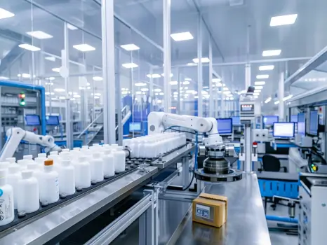
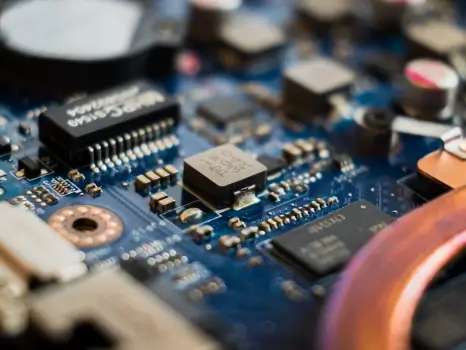
High-end electronics manufacturing (wafer, chip, panel display, new energy) faces multiple core challenges:
- Particulate and chemical-contamination risk: In critical process steps such as photolithography, etching, diffusion and packaging, both particulate matter and airborne molecular contamination (AMC)—including acids and bases, VOCs and dopant gases—can severely erode product yield and reliability.
- Pressure from ever-tightening process precision: As chip process nodes rapidly scale down and display resolution keeps climbing, the requirements for filtration precision and stability far exceed conventional industrial standards, so traditional “off-the-shelf specifications” can no longer meet real-world operating conditions.
- Conflict between energy consumption and operating cost: Over long-term operation, filtration systems suffer rapid pressure-drop rise and frequent maintenance, keeping power consumption and replacement cost persistently high—in direct conflict with green-manufacturing goals.
The LANSIR Solution
Following the principle of ‘customizing to stricter performance specifications’, LANSIR delivers a systematic response strategy:
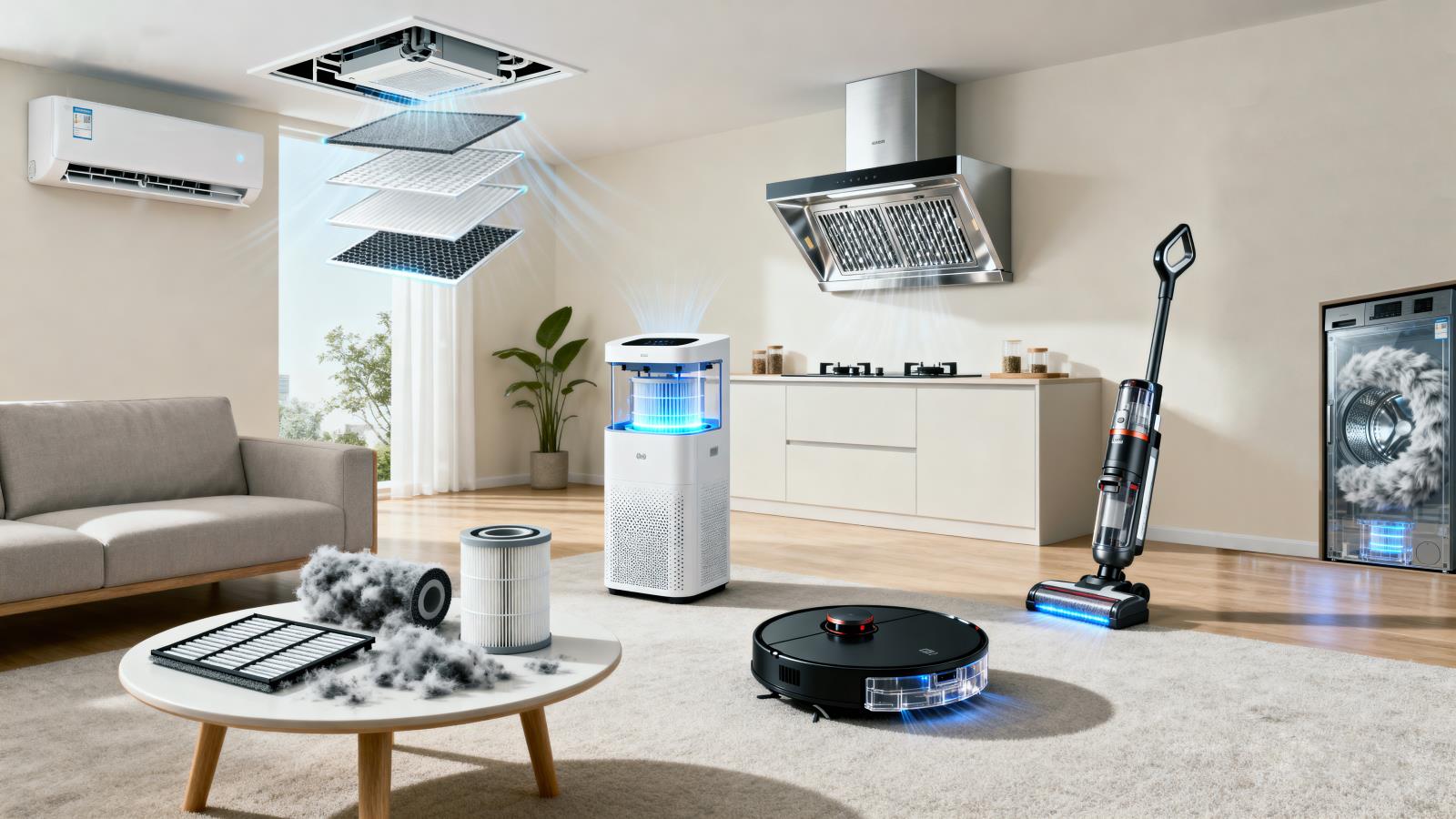
- Full-chain pollutant control: Precision filtration solutions covering everything from nano-scale particulate matter to AMC, and drawing on decades of field experience with diverse acids/bases, VOCs and dopant gases, effectively safeguard process-environment cleanliness (cleanroom classification per ISO 14644-1).
- Performance and energy savings combined: We engineer our products for sustained high efficiency, stable pressure drop and extended service life, while an energy-saving design markedly reduces power consumption and lowers long-term operating expense (OPEX)—balancing economic benefit with environmental benefit.
- Rejecting off-the-shelf standards: Rather than adopting generic industry specifications, we customize exclusive performance specifications to each customer’s actual operating conditions, ensuring stable and reliable performance even in the most demanding steps such as photolithography, etching and diffusion. We have validated the solution across multiple generations of process-node iterations.
Application Scenarios
Semiconductor front-end; advanced packaging; panel display; new energy; lithium battery material preparation; fuel cell membrane electrode assembly processing; electrolyte purification, and other emerging scenarios